LinkSys EA6100 AC1200 - Part 2 - A serial connection FTW!


Last time we left off with a pretty decent understanding about how our router is structured and what components were used. We also found two interesting debug pads that showed oscillating voltages during boot up. In this post, we will take a closer look at exactly these and try to get a Read-Write serial connection going. The goal this time will be to be able to analyze the firmware on the device and being able to decrypt the image we've seen earlier!
Recap:
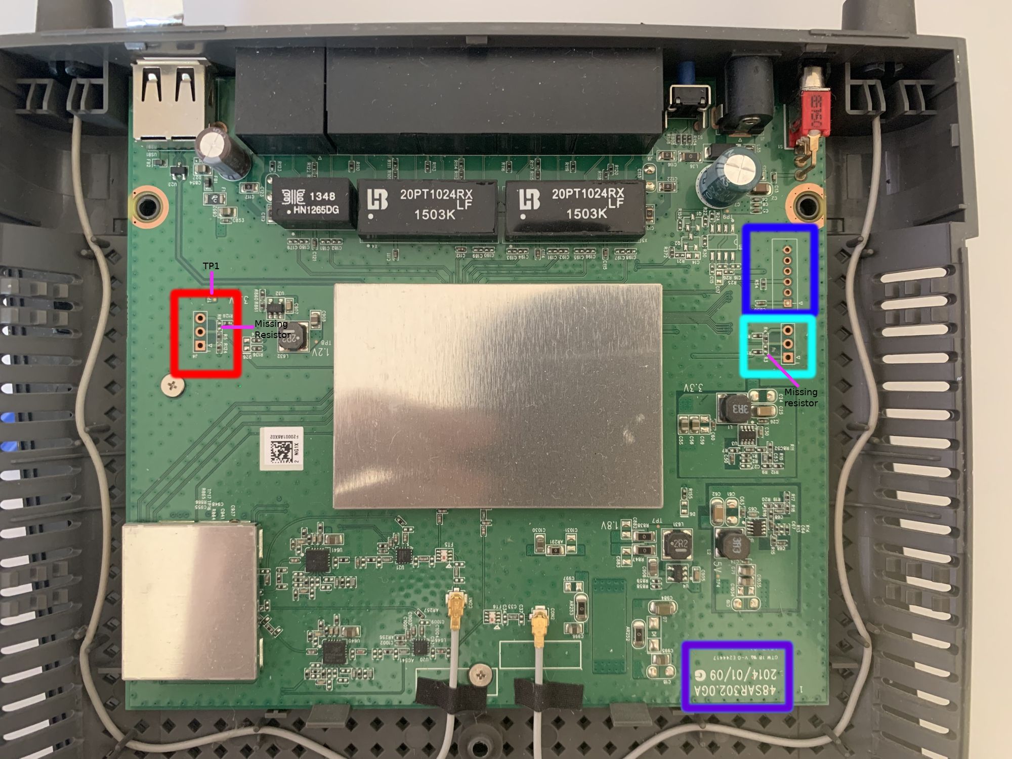
The two oscillating voltages we were able to measure with our multi meter last time around were on pin 2 (turquoise box) and pin 5 (blue box). The left side (red box) did not look that promising at first. Let's first verify what these oscillating voltages actually are and, if they are indeed transmitting data, whether they are the same or actually different! I noticed that following along with only the PCB pictures is tough, so here is a schematic of how far we progressed last time:
                                                                                     +--+
                                                 +--+                                |  |  Pin 6: 0V (GND!)
                   +--+              TP 2: 3.3V  |  |                                +--+
       TP 1: 3.3V  |  |                       +-----+                                |  |  Pin 5: Oscillating (TX?)
                   +--+           TP 3: 3.3V  |  |                                   +--+
                                              +--+                                   |  |  Pin 4: 0V
                                                                                     +--+
             +--+                                                                    |  |  Pin 3: 0V
Pin 3: 0V    |  |                        +----------------+   +-----+                +--+
             +--+                        |                |   |     |                |  |  Pin 2: 0V
Pin 2: 3.3V  |  +----+                   |                |   |     |                +--+
             +--+    |                   |                |   |     |                |  |  Pin 1: 3.3V (VCC?)
Pin 1: 3.3V  |  +<---+                   |                |   |     |                +--+
             +--+                        |      CPU       |   | RAM |
                                         |                |   |     |                +--+
                                         |                |   |     |           +----+  |  Pin 3: Oscillating (TX?)
                                         |                |   |     |           |    +--+
                                         |                |   |     |           +--->+  |  Pin 2: Oscillating (TX?)
                                         |                |   |     |                +--+
                                         +----------------+   +-----+                |  |  Pin 1: 3.3V
                                                                                     +--+
I hope this diagram will help you follow along. Now let's try to confirm these 3 potential transmit pins (TX). We're starting with the 6 pin row. After some quick and dirty soldering, the backside of the router now looks like this:
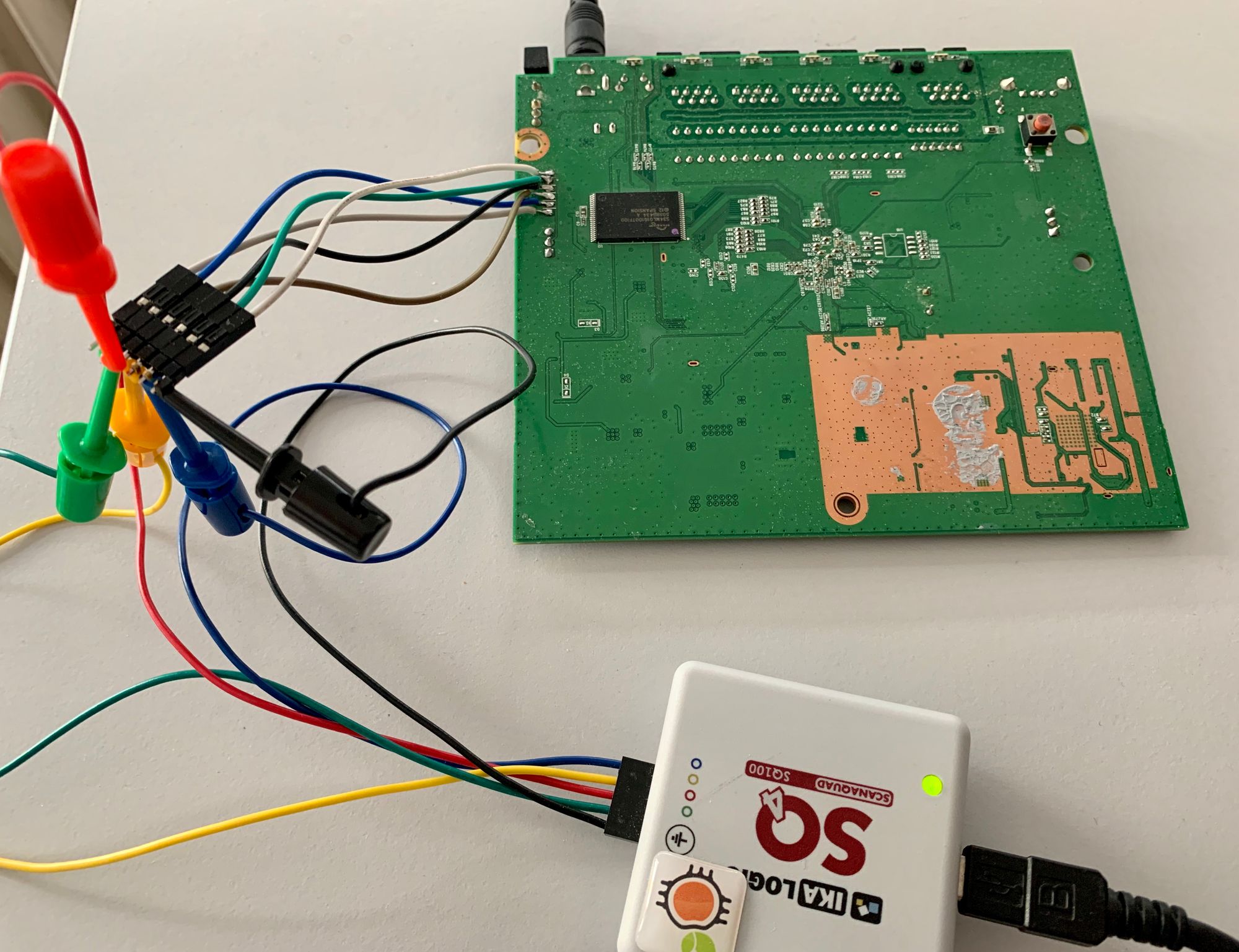
For the two rows with 3 through holes each, I quickly soldered some 2.54 mm headers on them. The row with 6 through holes were too small to fit the 2.54 mm ones, so I had to resort to using some cables... When powering on the device, a short signal capture allows us to peak at the signal curve:
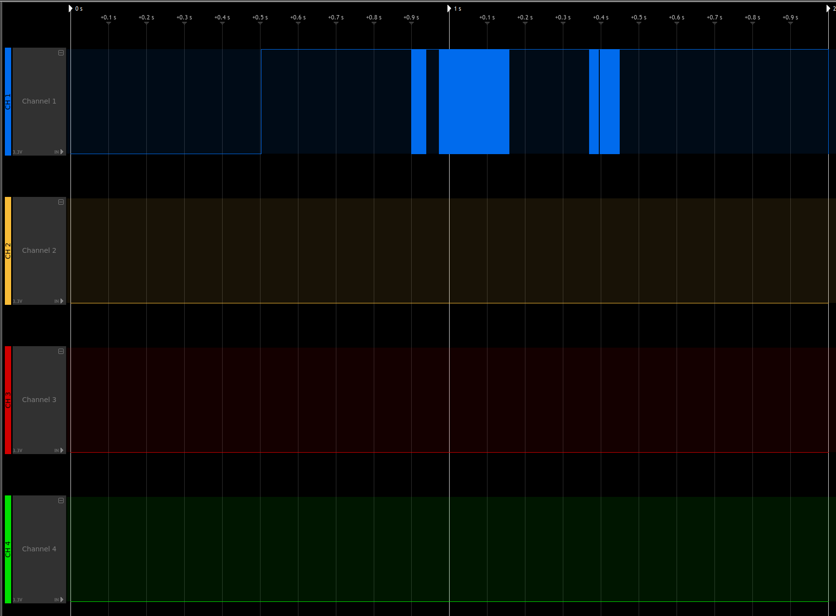
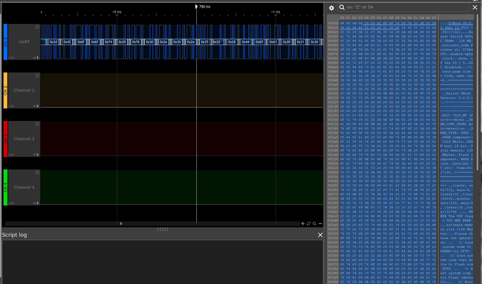
When decoding channel 1 (CH1, blue) with the included UART protocol decoder on default settings and a baudrate of 57600 our signal is perfectly 'translated' to a human-readable ASCII format (on the right). I was only able to capture about roughly 2 seconds, as my logic analyzer at that time could not handle more (sad noises). However, the short capture already gives plenty of insight:
- This pin 5 is actually transmitting data
- The device uses UBoot v0.0.5
- The board is a Ralink one
- We have 128 MB of RAM (known to us already!)
- Suddenly Ralink Uboot v4.2.S.1 takes over
- CPU Freq is at 580Mhz (known to us already!)
- There is an Uboot menu with at least 4 options
-
- Load system code to SDRAM via TFTP
-
- Load system code then write to Flash via TFTP
-
- Boot system code via Flash (default)
-
- Entr...?
-
First, are we dealing with a two stage bootloader variant here? Unlikely! It's more likely that Ralink pulled the ancient Uboot v0.0.5 from the official sources, and they modified it to their needs, which results in v4.2.S.1 for their internal bookkeeping. So, what about the other two pins that also showed oscillating voltages?
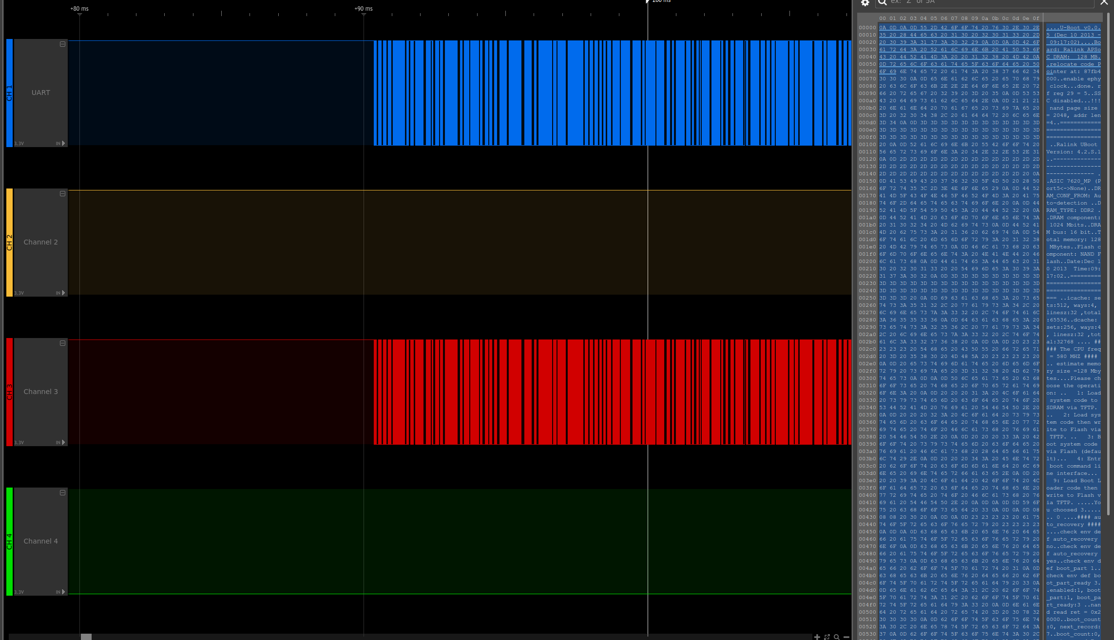
They actually as TX lines as well (as we suspected). What we get by confirming this is the fact that actually have the same Uboot bootloader stdout log on these two pins. Also, the signal clearly shows that these two pins are identical (just visually compare them!). Finally, as I started capturing a little later, we also get an idea what post Uboot bootloader option 4 is happening:
- There is an Uboot menu with at least 4 options
- ...
-
- Entr boot command line interface
-
- Load Boot loader code then write to Flash via TFTP
This allows us to update our ground truth in the ASCII diagram just slightly but every piece of knowledge brings us closer to our goal!
                                                                                     +--+
                                                 +--+                                |  |  Pin 6: GND
                   +--+              TP 2: 3.3V  |  |                                +--+
       TP 1: 3.3V  |  |                       +-----+                                |  |  Pin 5: TX
                   +--+           TP 3: 3.3V  |  |                                   +--+
                                              +--+                                   |  |  Pin 4: 0V
                                                                                     +--+
             +--+                                                                    |  |  Pin 3: 0V
Pin 3: 0V    |  |                        +----------------+   +-----+                +--+
             +--+                        |                |   |     |                |  |  Pin 2: 0V
Pin 2: 3.3V  |  +----+                   |                |   |     |                +--+
             +--+    |                   |                |   |     |                |  |  Pin 1: 3.3V
Pin 1: 3.3V  |  +<---+                   |                |   |     |                +--+
             +--+                        |      CPU       |   | RAM |
                                         |                |   |     |                +--+
                                         |                |   |     |           +----+  |  Pin 3: TX
                                         |                |   |     |           |    +--+
                                         |                |   |     |           +--->+  |  Pin 2: TX
                                         |                |   |     |                +--+
                                         +----------------+   +-----+                |  |  Pin 1: 3.3V
                                                                                     +--+
Finding GND and TX is the easy part. We still have to identify at least VCC, RX pins, potentially even a clock signal, reset line and others depending on the serial connection we're aiming for. That
If we assume that VCC pins, used for powering components rely on having fatter traces on the PCB due to needing to transfer enough voltage with them, most likely be connected to a capacitor for storing some of this electrical energy we have a natural candidate for a VCC pin. Pin 1 of the 6 pin connector on the right side of the PCB. From this assumption, we can also derive the fact that when powering off the device VCC pins should discharge slower, or in other words not hit 0V right away! I've tested this on all the not yet identified pins that showed a constant 3.3V when the device is powered on. Unfortunately, all the pins showed the same symptoms. After powering off the device, the voltages about instantly dropped to around 300mV and then very slowly discharged further from there. This would indicate that all of them are VCC pins. If we apply this to our diagram above, it changes as follows:
                                                                                     +--+
                                                 +--+                                |  |  Pin 6: GND
                   +--+              TP 2: VCC   |  |                                +--+
       TP 1: VCC   |  |                       +-----+                                |  |  Pin 5: TX
                   +--+           TP 3: VCC   |  |                                   +--+
                                              +--+                                   |  |  Pin 4: 0V
                                                                                     +--+
             +--+                                                                    |  |  Pin 3: 0V
Pin 3: 0V    |  |                        +----------------+   +-----+                +--+
             +--+                        |                |   |     |                |  |  Pin 2: 0V
Pin 2: VCC   |  +----+                   |                |   |     |                +--+
             +--+    |                   |                |   |     |                |  |  Pin 1: VCC
Pin 1: VCC   |  +<---+                   |                |   |     |                +--+
             +--+                        |      CPU       |   | RAM |
                                         |                |   |     |                +--+
                                         |                |   |     |           +----+  |  Pin 3: TX
                                         |                |   |     |           |    +--+
                                         |                |   |     |           +--->+  |  Pin 2: TX
                                         |                |   |     |                +--+
                                         +----------------+   +-----+                |  |  Pin 1: VCC
                                                                                     +--+
At this point, the VCC pins are not fully verified but if our labeling is going to turn out to be correct we just need to finish identifying those 4 pins that are at 0V.
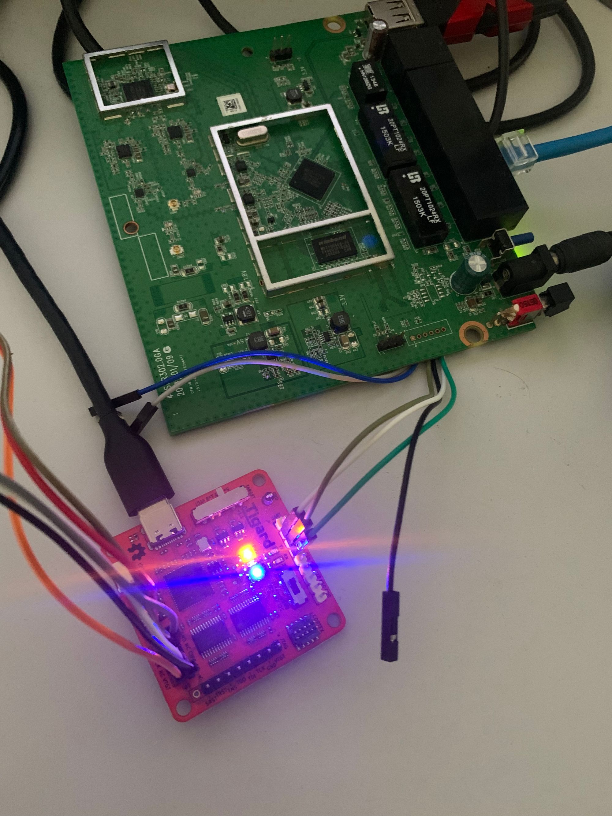
With some trial and error while still being connected to the boot console via UART with our known TX and GND pins I was able to deduct that on the larger header on the right, Pin 3 is indeed a RX pin as I was able to type at one point during the boot process. The wiring was done with my trusty pal the Tigard:
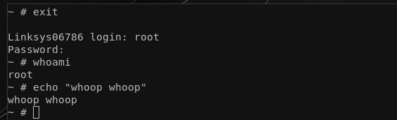
With that out of the way, let's enter the device:
The UART prompt has a super secure login protection :p. For those of you who have watched the recording above, you saw me trying the first credentials coming to mind... Why bother enabling a prompt when the credentials are admin:admin? Who knows... With that said, we're the admin user at this point but actually not the root user!
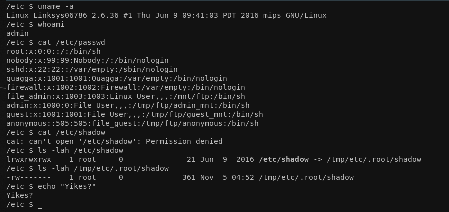
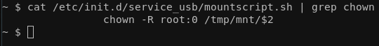
Now with the admin user, we're pretty restricted as all important files like the real /etc/shadow are only accessible by the root user, while many files in /etc have the same behavior of simply being a symlink to the /tmp directory and hence only being writable by root:
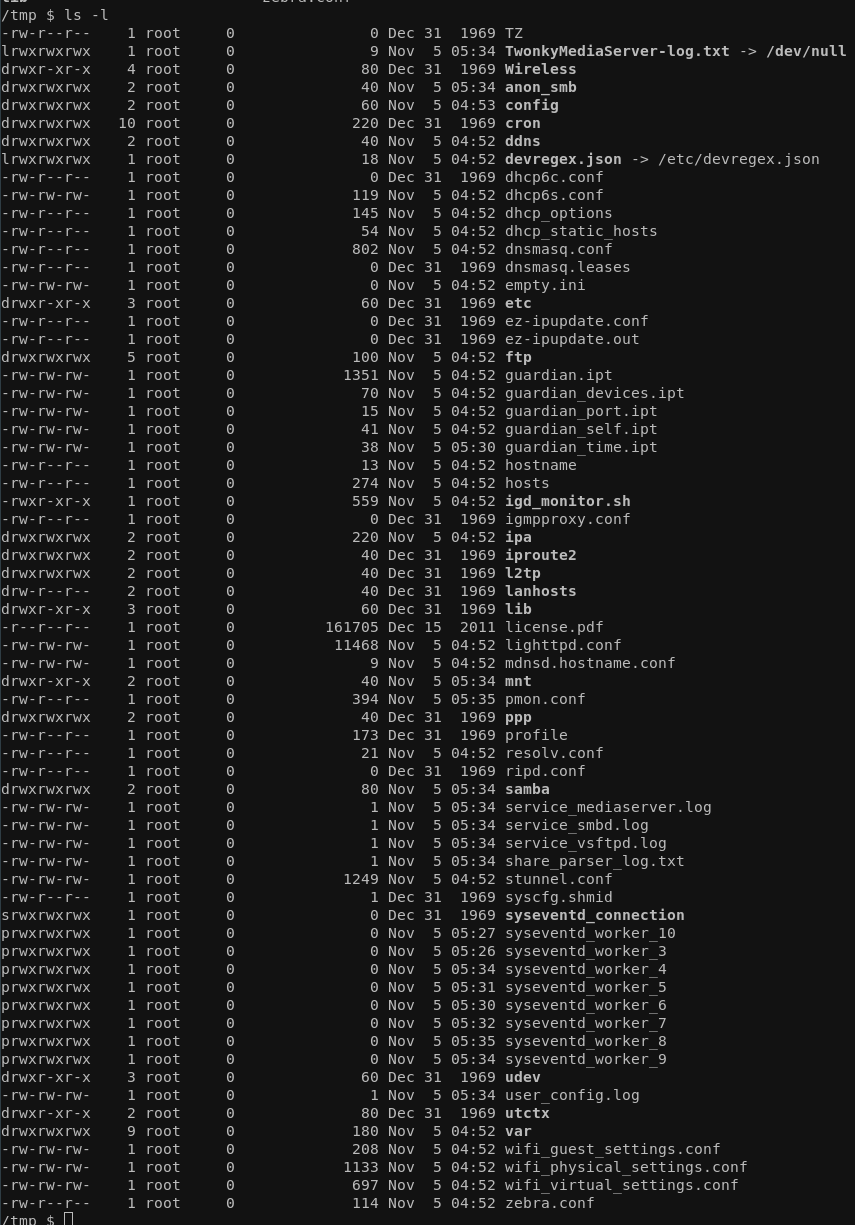
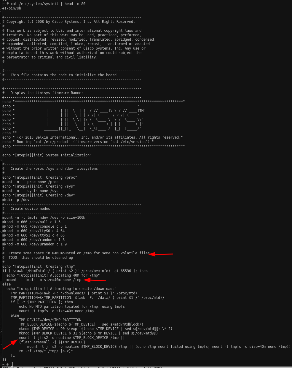
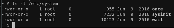
The reason for it being that way should be clear. Most if not all config related files are stored in some separate file system that is being dynamically mounted during boot-up. We can see how and why in the /etc/inittab:
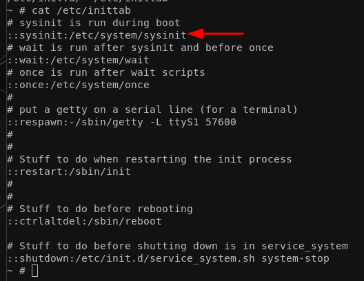
Following inittab and with that, the /etc/system/once and /etc/system/wait we can learn a ton more about the initialization routine and especially about why the system behaves the way it behaves and where the configuration comes from. However, we're still stuck as the admin user, so we couldn't manipulate the current behavior even if we wanted to:
At this point, I wanted to dump the file system to a USB drive and go from there but even though external USB devices are automatically mounted they're always mounted as only writable from root (copying from the USB drive to the device works just fine as any user though).
Then I took a step back and thought, what if the root user login is as trivial as the admin one? I was grepping around the file system to see if some obvious root user configuration takes place, and what can I say... Look for yourself:
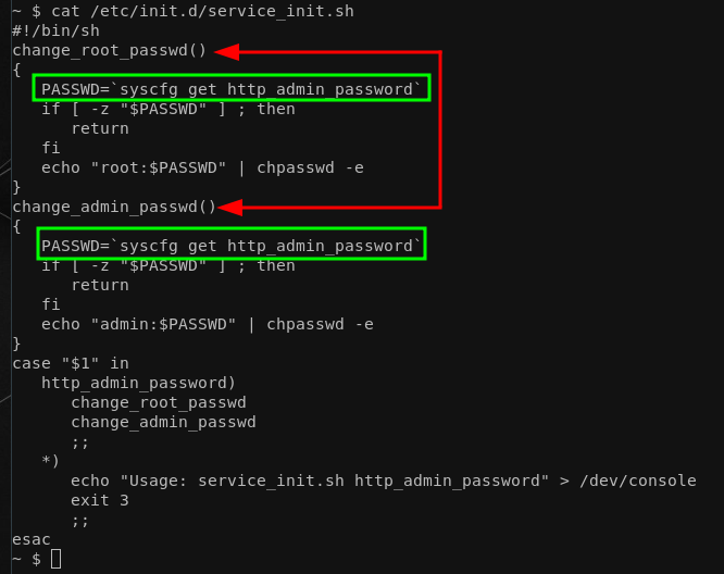
Like what? Being at this point, it does not even matter where http_admin_password comes from as it's the same for both admin and root. For completeness, all defaults that are initialized during boot are stored in /etc/system_defaults:

I'll just leave this here, in case you're wondering what "TSLIIHauhEfGE" is.
With that out of the way, we can also dump the file system to an external USB drive without worrying (alternative ways like using nc or the tftp which are present on the device per default would have worked too). So for the final task, let's figure out the firmware update process! Having access to the rootfs locally helped immensely. Grepping for a few obvious candidates again reveals the likeliest candidates where firmware updates are handled:
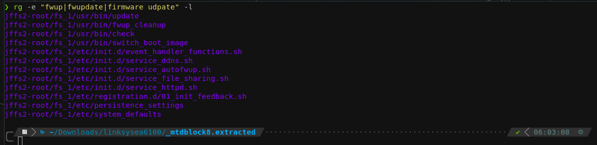
Long story short, the magic happens /etc/init.d/service_autofwup.sh. Here are the most interesting bits of the file:
#!/bin/sh
source /etc/init.d/interface_functions.sh
source /etc/init.d/ulog_functions.sh
source /etc/init.d/event_handler_functions.sh
SERVICE_NAME="autofwup"
Debug()
{
	echo "[FW.sh] $@" >> /dev/console
}
check_dual_partition_update()
{
	FIRMWARE_PART_1=`syscfg get fwup_part_1`
	FIRMWARE_PART_2=`syscfg get fwup_part_2`
	Debug "Checking dual partition update: $FORCED_UPDATE"
	Debug "part1: $FIRMWARE_PART_1"
	Debug "part2: $FIRMWARE_PART_2"
	if [ "$FORCED_UPDATE" == "$FIRMWARE_PART_1" ] && [ "$FORCED_UPDATE" == "$FIRMWARE_PART_2" ]; then
		Debug "Forced Update Done"
		PartitionUpdated=2
	fi
}

# [...]

verify_linksys_header ()
{
	ErrorCode=2
	Debug "verify_linksys_header"

	LINKSYS_HDR="/tmp/linksys.hdr"
	FILE_LENGTH=`stat -c%s "$1"`
	IMAGE_LENTGH=`expr "$FILE_LENGTH" - 256`
	dd if="$1" of="$LINKSYS_HDR" skip="$IMAGE_LENTGH" bs=1 count=256 > /dev/console
	magic_string="`cat $LINKSYS_HDR | cut -b 1-9`"
	if [ "$magic_string" != ".LINKSYS." ]
	then
		ulog autofwup status  "Fail : verify magic string "
		exit $ErrorCode
	fi
	hdr_version="`cat $LINKSYS_HDR | cut -b 10-11`"
	hdr_length="`cat $LINKSYS_HDR | cut -b 12-16`"
	sku_length="`cat $LINKSYS_HDR | cut -b 17`"
	sku_end=`expr 18 + "$sku_length" - 2`
	sku_string="`cat $LINKSYS_HDR | cut -b 18-$sku_end`"
	img_cksum="`cat $LINKSYS_HDR | cut -b 33-40`"
	sign_type="`cat $LINKSYS_HDR | cut -b 41`"
	signer="`cat $LINKSYS_HDR | cut -b 42-48`"
	kernel_ofs="`cat $LINKSYS_HDR | cut -b 50-56`"
	rfs_ofs="`cat $LINKSYS_HDR | cut -b 58-64`"
	crc1=`dd if="$1" bs="$IMAGE_LENTGH" count=1| cksum | cut -d' ' -f1`
	hex_cksum=`printf "%08X" "$crc1"`
	if [ "$img_cksum" != "$hex_cksum" ]
	then
		ulog autofwup status "Fail : verify image checksum "
		Debug "Checksum Error"
		exit $ErrorCode
	fi

	Debug "verify_linksys_header: success"
}

verify_header ()
{
	header_file="/tmp/img_hdr"
	magic="`cat $header_file | cut -b 1-6`"
	version="`cat $header_file | cut -b 7-8`"
	img_cksum="`cat $header_file | cut -b 25-32`"
	rm -rf $header_file
	if [ "$magic" != ".CSIH." ]
	then
		ulog autofwup status "Fail : verify magic "
		exit 1
	fi

	if [ "$version" != "01" ]
	then
		ulog autofwup status "Fail : verify version "
		exit 1
	fi
	crc1=`cksum $1 | cut -d' ' -f1`
	hex_cksum=`printf "%08X" "$crc1"`
	if [ "$img_cksum" != "$hex_cksum" ]
	then
		ulog autofwup status "Fail : verify checksum "
		exit 1
	fi
}

update_key_data()
{
	Server=$(syscfg get fwup_server_uri)
	Model=$(syscfg get device::modelNumber)
	Hardware=$(syscfg get device::hw_revision)
	Mac=$(syscfg get device::mac_addr | tr -s ':' '-')
	Version=$(syscfg get fwup_firmware_version)
	Serial=$(syscfg get device::serial_number)
	Request=$(printf "%s/api/v2/key?manufacturer=linksys&mac_address=%s&model_number=%s&hardware_version=%\
    s&installed_version=%s&serial_number=%s" $Server $Model $Hardware $Mac $Version $Serial)
	KeyData1=/var/config/keydata
	KeyData2=/etc/keydata
	echo "$Request"
	if [ -e "$1" ]; then
		rm "$1"
	fi
	Response="$1.dat"
	curl --capath "/etc/certs/root" -o "$Response" "$Request"
	if [ $? -eq 0 ] && [ -s "$Response" ]; then
		fwkey "$Response" "$1"
	else
		Debug "updating key: failed"
	fi
	if [ -s "$1" ]; then
		diff -q "$1" "$KeyData1"
		if [ $? -ne 0 ]; then
			cp "$1" "$KeyData1"
		fi
	else
		if [ -s "$KeyData1" ]; then
			cp "$KeyData1" "$1"
		else
			if [ -s "$KeyData2" ]; then
				cp "$KeyData2" "$1"
			fi
		fi
	fi
}
check_gpg_signature()
{
	Error=2
	Debug "check_gpg_signature"
	export GNUPGHOME=/tmp/gpg
	if [ ! -d $GNUPGHOME ]; then
		mkdir $GNUPGHOME
		chmod 700 $GNUPGHOME
	fi
	cd $GNUPGHOME
	KeyData="$GNUPGHOME/keydata"
	update_key_data $KeyData
	gpg --import --ignore-time-conflict "$KeyData"
	if [ $? -ne 0 ]; then
		return $Error
	fi
	gpg --verify --ignore-time-conflict "$1"
	if [ $? -ne 0 ]; then
		return $Error
	fi

	Debug "check_gpg_signature: success"
}

decrypt_gpg_image()
{
	Error=2
	Debug "decrypt_gpg_image"
	ImageFile="$GNUPGHOME/firmware"
	gpg --ignore-time-conflict -d "$1" > $ImageFile

	if [ $? -ne 0 ]; then
		return $Error
	fi
	FirmwareImage="$ImageFile"
	Debug "decrypt_gpg_image: success"
}
extract_gpg_image()
{
	Error=2
	check_gpg_signature "$1"

	if [ $? -ne 0 ]; then
		return $Error
	fi
	decrypt_gpg_image "$1"
	if [ $? -ne 0 ]; then
		return $Error
	fi
}

check_signature()
{
	ErrorCode=2
	Debug "check_signature [$1]"
	if [ ! -e "$1" ]; then
		exit $ErrorCode
	fi
	check_gpg_signature "$1"
	if [ $? -ne 0 ]; then
		verify_linksys_header "$1"
	fi
}
verify_signature()
{
	ErrorCode=2
	Debug "verify_signature [$1]"
	if [ ! -e "$1" ]; then
		exit $ErrorCode
	fi
	RegionCode=`skuapi -g cert_region | awk -F"=" '{print $2}' | sed 's/ //g'`
	ProdType=$(cat /etc/product.type)
	GpgMode=$(syscfg get fwup_gpg_mode)
	extract_gpg_image "$1"
	if [ $? -ne 0 ]; then
		FirmwareImage=""
	fi
	if [ "$FirmwareImage" == "" ]; then
		if [ "$RegionCode" == "US" ] && [ "$ProdType" == "production" ]; then
			exit $ErrorCode
		elif [ "$GpgMode" == "1" ]; then
			exit $ErrorCode
		else
			FirmwareImage="$1"
		fi
	fi
}

# [...]
Ultimately, there are a few interesting bits and pieces like the verify(_linksys)_header functions where we can exactly see which bytes in the raw data correspond to what field in the header. That said, what we need to decrypt our official firmware update from part1, namely FW_EA6100_1.1.6.181939_prod.gpg.img are the couple of gpg related functions! Our decryption routine roughly looks as follows now:
GNUPGHOME=/tmp/gpg
KeyData="$GNUPGHOME/keydata"
gpg --import --ignore-time-conflict "$KeyData"
gpg --ignore-time-conflict -d EncryptedFW > DecryptedFW
If we look closer, we're able to see that the content of KeyData is also dynamically generated by querying the system config contents via syscfg get <key> and if the new key data differs from the currently present key data we update it accordingly:
update_key_data()
{
	Server=$(syscfg get fwup_server_uri)
	Model=$(syscfg get device::modelNumber)
	Hardware=$(syscfg get device::hw_revision)
	Mac=$(syscfg get device::mac_addr | tr -s ':' '-')
	Version=$(syscfg get fwup_firmware_version)
	Serial=$(syscfg get device::serial_number)
	Request=$(printf "%s/api/v2/key?manufacturer=linksys&mac_address=%s&model_number=%s&hardware_version=%s\
    &installed_version=%s&serial_number=%s" $Server $Model $Hardware $Mac $Version $Serial)
	KeyData1=/var/config/keydata
	KeyData2=/etc/keydata
	echo "$Request"
	if [ -e "$1" ]; then
		rm "$1"
	fi
	Response="$1.dat"
	curl --capath "/etc/certs/root" -o "$Response" "$Request"
	if [ $? -eq 0 ] && [ -s "$Response" ]; then
		fwkey "$Response" "$1"
	else
		Debug "updating key: failed"
	fi
	if [ -s "$1" ]; then
		diff -q "$1" "$KeyData1"
		if [ $? -ne 0 ]; then
			cp "$1" "$KeyData1"
		fi
	else
		if [ -s "$KeyData1" ]; then
			cp "$KeyData1" "$1"
		else
			if [ -s "$KeyData2" ]; then
				cp "$KeyData2" "$1"
			fi
		fi
	fi
}
At the time of writing, this article, $Request holds this value for me: https://update1.linksys.com/api/v2/key?manufacturer=linksys&mac_address=EA6100-EU&model_number=1&hardware_version=<redacted>&installed_version=1.1.6.173444&serial_number=<redacted>. Curling this API endpoint works and returns the needed GPG key:
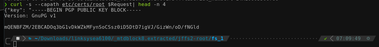
Putting it all together enables us to fully decrypt the new firmware and start analyzing that one as well. The number of devices for which this encryption scheme with the same GPG key works is yet to be tested:
And with that, we're already coming to an end here. Analyzing the whole firmware image is out of scope for this article, but maybe we can take a look at a later time :) (Hit me up if you're interested). To summarize, in this little blog post series, we:
- Learned some PCB reversing,
- Reviewed some UART basics,
- Gained some more insight into how firmware updates for IoT devices could potentially be delivered securely (at least to some degree),
- We peeked at how
init.dis used for system initialization, and finally - We saw how to use QEMU locally to utilize our firmware dump that has a different architecture effectively.
Note: This blog post is purely for educational purposes and does not highlight anything new or groundbreaking. It's mostly for my little archive and if anyone finds it interesting to read or even learns just a tiny bit, putting it out here was the right choice.
P.S.: I'm fully aware that this is a thing and LinkSys apparently failed to properly delivery GPG encrypted firmware images from the start, so they had to put this huge disclaimer there and provide two firmware samples, one unencrypted that contains the GPG key and the newer encrypted ones. Also, don't ask me why that's only true for the US region but not the "other regions":