It has been a while since I did some hardware hacking, and this time I want to review the basics. The LinkSys EA6100 router intrigued me since I was only able to find encrypted firmware images (or updates). Known tools like binwalk were unable to unpack the system:
> file FW_EA6100_1.1.6.181939_prod.gpg.img
FW_EA6100_1.1.6.181939_prod.gpg.img: data
> md5sum FW_EA6100_1.1.6.181939_prod.gpg.img
25efc5b63d6b35366bf556111d0a8368  FW_EA6100_1.1.6.181939_prod.gpg.img
> binwalk FW_EA6100_1.1.6.181939_prod.gpg.img

DECIMAL       HEXADECIMAL     DESCRIPTION
--------------------------------------------------------------------------------
30445         0x76ED          MySQL MISAM index file Version 2

> binwalk -E FW_EA6100_1.1.6.181939_prod.gpg.img

DECIMAL       HEXADECIMAL     ENTROPY
--------------------------------------------------------------------------------
0             0x0             Rising entropy edge (0.998097)

The official firmware update instructions state that you can download this file above and upload it to your router via the web interface. The firmware updates automatically when the upload is successful. As a result of me being interested in what these firmware files actually contain, I got my hands on one of these devices.
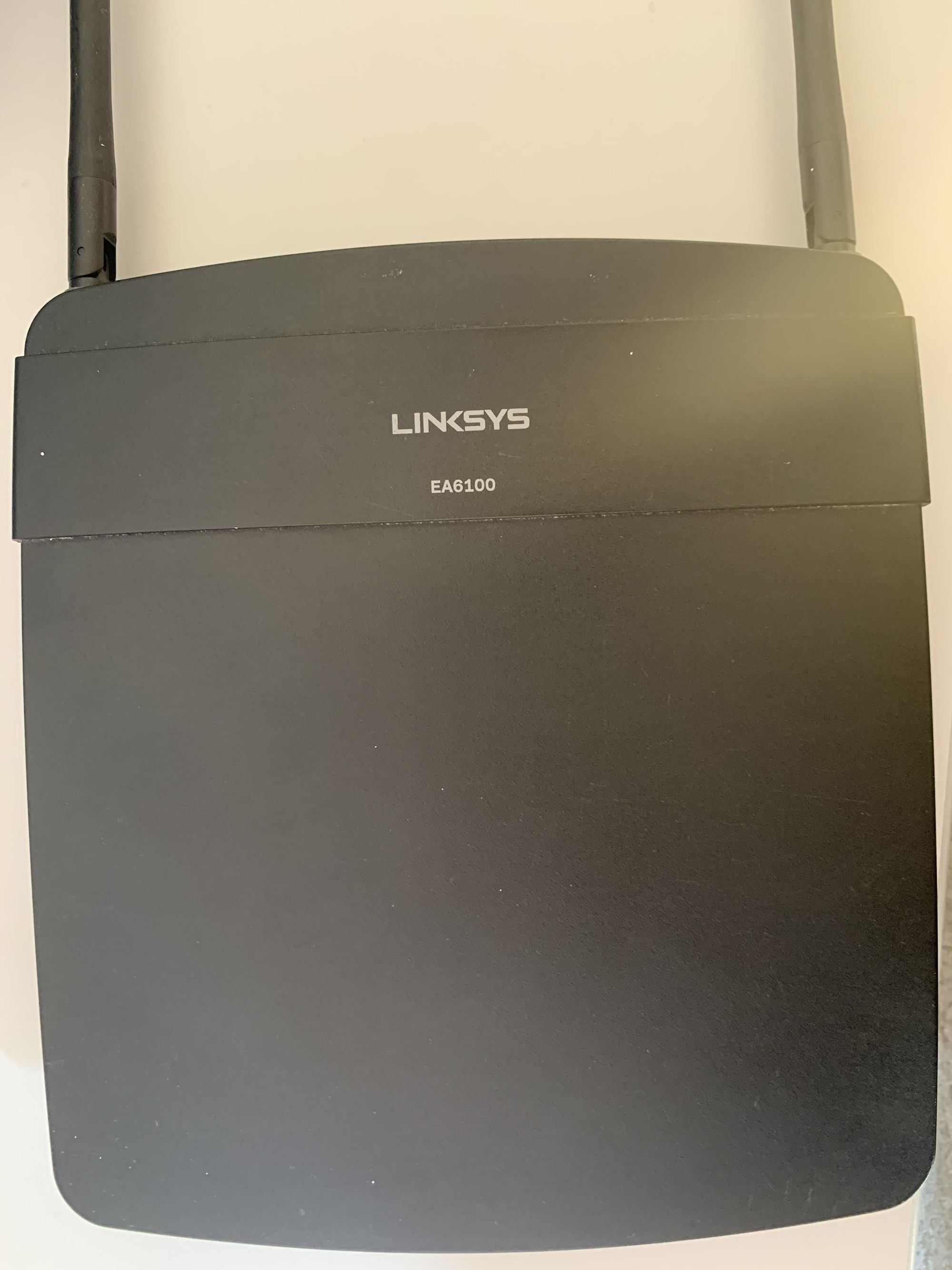
From the outside it looks nothing like the modern spaceships models, but as we all know it is the inner values that count :). After cracking open the case, I was greeted with the following:
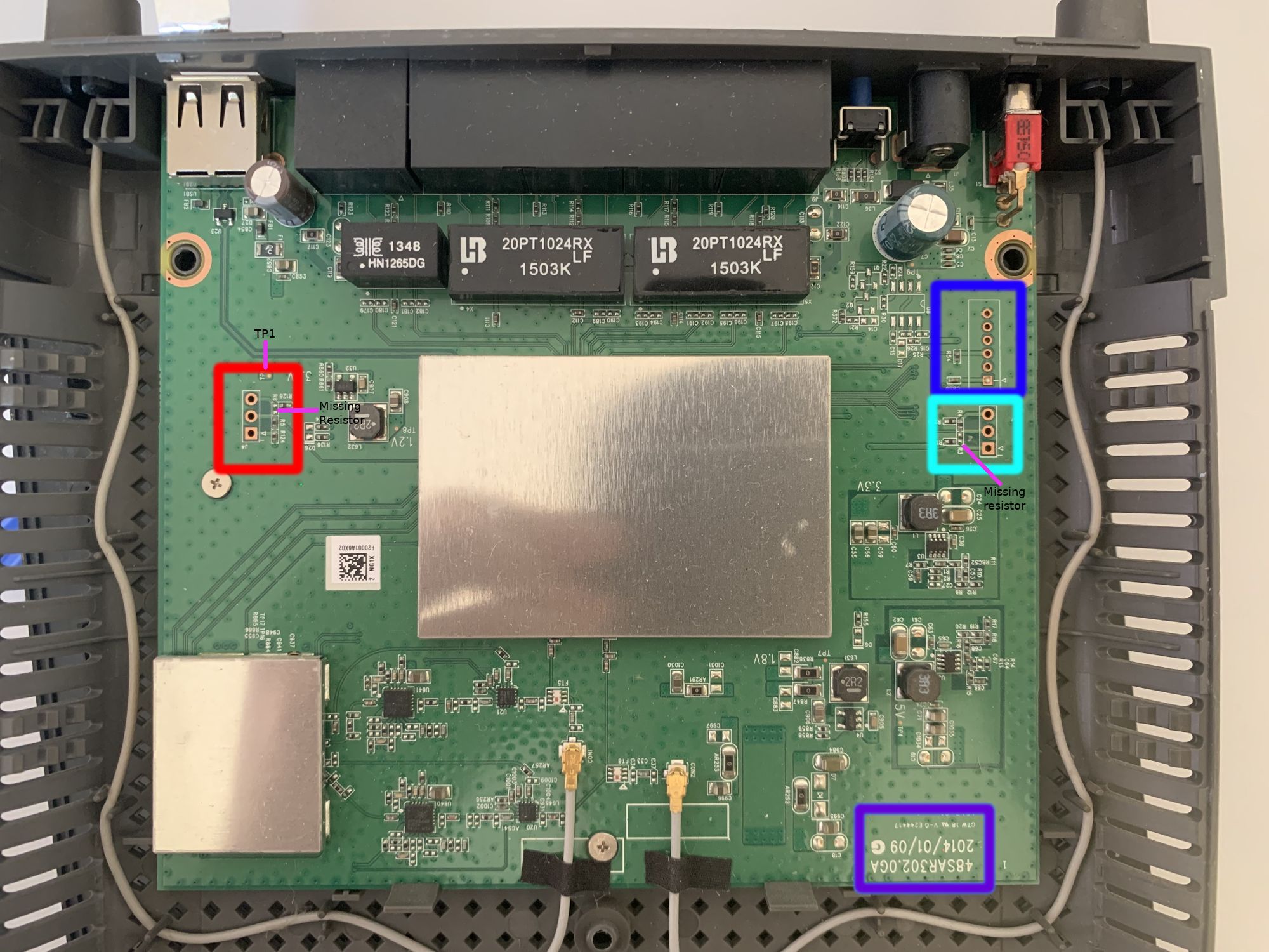
The first thing one can notice are the two shields covering most of the interesting bits of the PCB. However, there is still plenty to work with:
- Purple box - Here we can see a label silkscreened onto the PCB. These often can lead to interesting facts from the manufacturer. In this case I could only find 3 identical wiki entries with only some additional information. Nevertheless, these wiki entries contain chip names for the CPU, RAM, Flash memory and WIFI:
- CPU - MediaTek MT7620A
- Flash - Spansion S34ML01G100TFI00
- RAM - Winbond W971GG6KB-25 (128 MB)
- WIFI - MediaTek MT7612E
We will confirm these as soon as we pop of the shields!
- Red Box - On the left side we got three through holes for a potential debug header pads labeled as J4 (J == connector jack). The square hole usually indicates Pin 1, which I will do as well for further labeling down the road. Additionally, something that may be also difficult to spot on the picture is that resistor 6 (R6) is missing (Maybe a hint?)! Using my multimeter I was able to observe the following behavior during boot up (from top to bottom):
- Pin 3 - 0V
- Pin 2 - 3.3V
- Pin 1 - 3.3V ; square one
Also there is a tiny copper via labeled TP1 above Pin 3, which is also at a constant 3.3V when the device is powered on.
- Turqois Box - At first glance this seems to be exactly mirrored from the one on the left, just with no silkscreen label. There is a similar pinout, similar traces, and there is also a resistor missing (R3) (Now it looks like a pattern already..). The multimeter reveals a different picture though. Again from top to bottom:
- Pin 3 - oscillating between ~0V - 3.3V
- Pin 2 - oscillating between ~0V - 3.3V
- Pin 1 - 3.3V ; square one
Oscillating voltages on such holes/pads during the boot up phase of a device are always a good sign as they indicate a transmitting signal. However, having two of these right next to each other is somewhat confusing... Then again when closely looking at the PCB one might notice that resistors R4 bridges the two, merging them into only one pin effectively.
- Blue Box - Lastly, this one has twice as many through holes available compared to the other two. It also has a silkscreen label (J2). Whipping out the multimeter a last time shows:
- Pin 6 - 0V
- Pin 5 - oscillating between ~0V - 3.3V ; see explanation earlier
- Pin 4 - 0V
- Pin 3 - 0V
- Pin 2 - 0V
- Pin 1 - 3.3V
When taking a second closer look at the PCB near the 6 pin connector, we can see that Pin 1 (bottom, square one) is hooked to a capacitor (C850) in addition to having a really fat trace going to it. This typically indicates that we're dealing with a VCC connection for supplying power to an IC here. Additionally, Pin 6 is connected to the ground plane indicated by the small "openings" around the pad to the left, top, and right side around it, meaning that it is GND (Try to look closely at the darker green parts around the copper pad). We can confirm this with the continuity test of the multi meter as well, which emits a beep sound when two points on a PCB are connected. In our case, we can use the USB port casing with the router in a powered off state and the potential GND pin to test our hypothesis. And indeed it is a GND pad.
This leaves us with 11 not yet fully identified pads plus an additional single TP1 via of which none are GND. However, 3 of those 11 seem to potentially transmit stuff that we could further analysis. Before that, let's flip the PCB upside down to check what we can see on the other side.
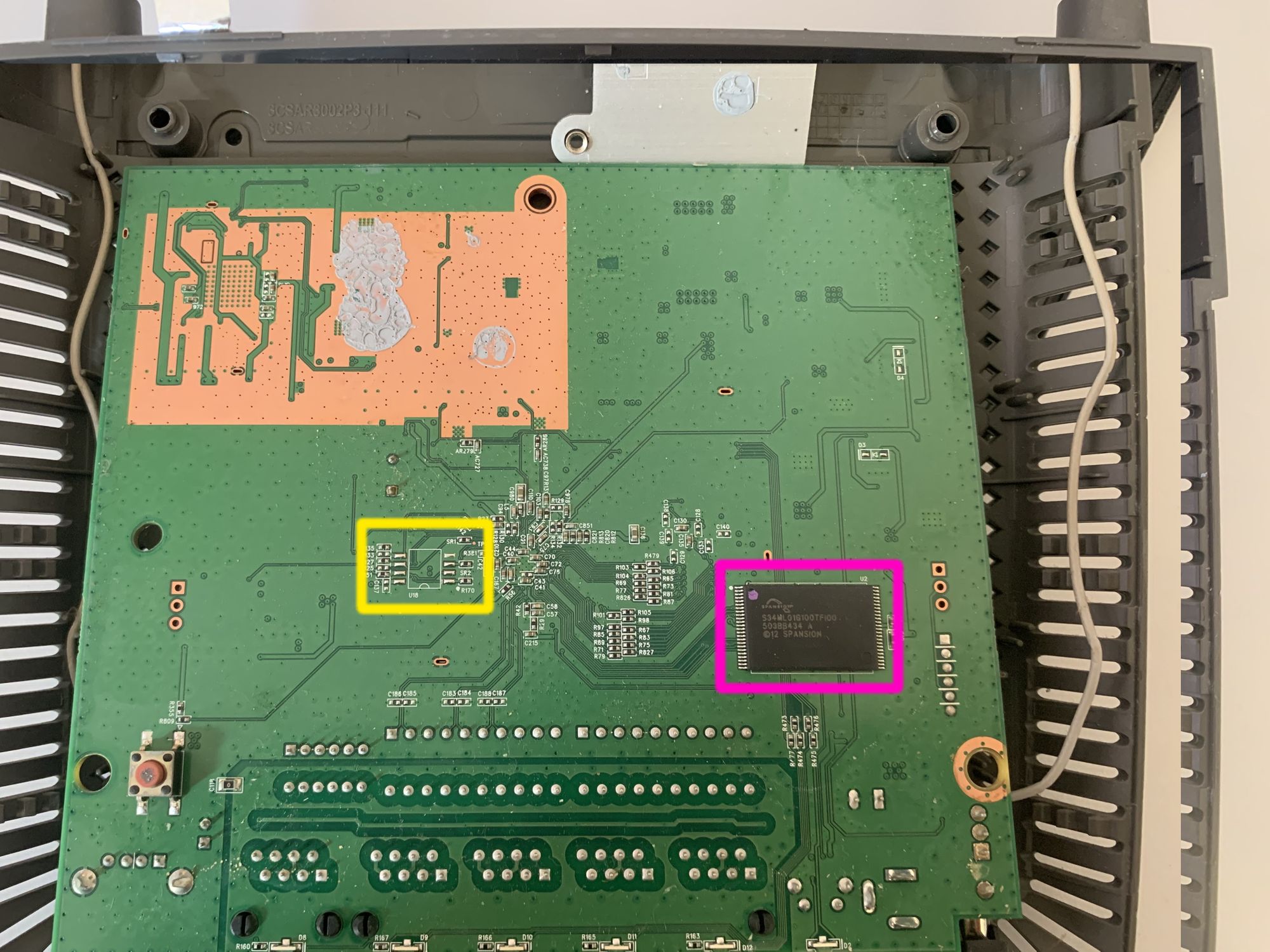
- Yellow box - Here we can see that the PCB is missing a potential SOIC8 chip. This could have been a potential target to read out memory contents via SPI as many of these chips support that.
- Pink box - Here we have a nice Spansion S34ML01G100TF100 128MB TSOP ("thin small-outline package") NAND flash memory. This is the same part number as stated in the earlier mentioned wiki, so there seems to be some truth to their part listings. The data sheet gives us a ton of information about how this chip operates, what its command set is, but also which pins are connected to what. To deepen our understanding of the PCB and with the new knowledge about the chip layout from the data sheet we can use the multi meter again and e.g.: check for GND/VCC pins of the NAND memory chip, as well as visually analyse where the traces from/to the chip are going! As an example just take the bottom 5 pins on the left side. The data sheet states they are not connected to anything. In this particular case we also cannot spot any traces on the top plane of the PCB, so that makes total sense!
That's it for the backside already... The large copper area at the top where even a solid piece of aluminum with solder paste was placed is most likely for the Wi-Fi chip to reduce noise and such. It's time to remove the shields!
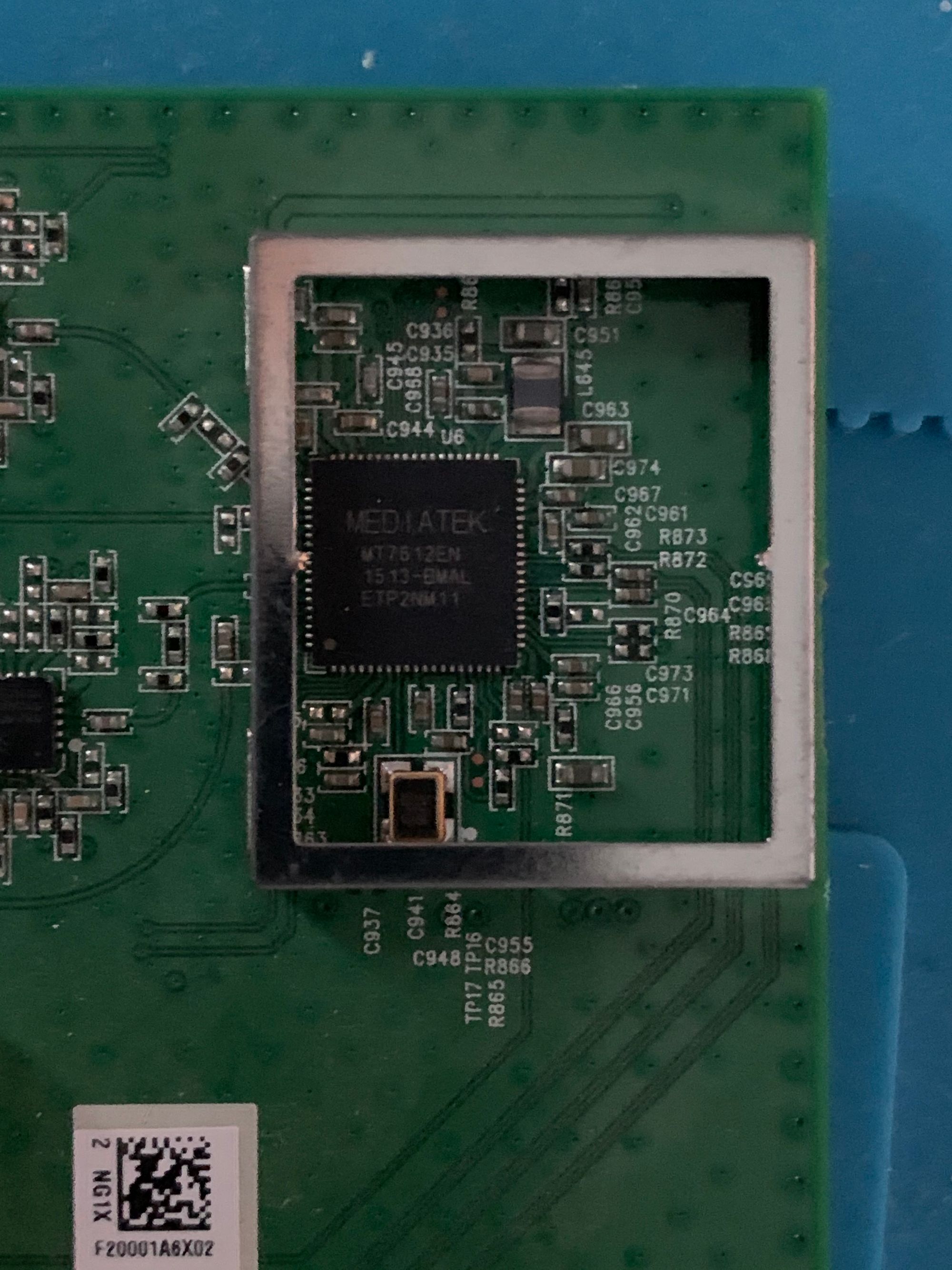
The small shield hides the Wi-Fi chip made by MediaTek. As this is no point of interest for us, we can just move on.
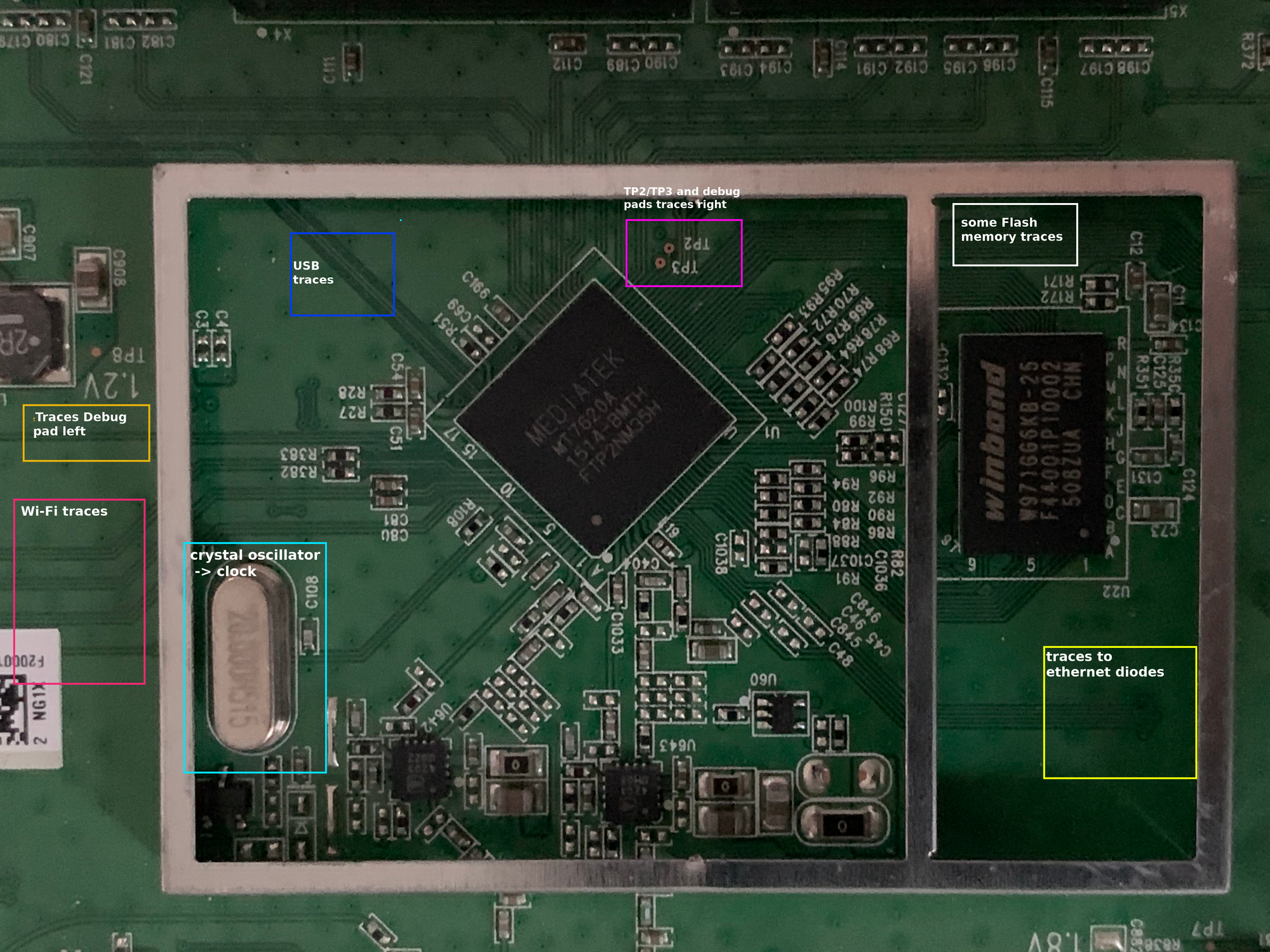
The larger shield was hiding another MediaTek chip. This time the CPU. The MT2620A is a 580 MHz MIPS router-on-a-chip. When looking at the data sheet, the feature list right at the beginning shows 2 very interesting bullet points:
- SPI, NAND Flash/SD-XC, and
- I2C, I2S, SPI, PCM, UART, JTAG, MDC, MDIO, GPIO
This means, that this architecture has support for most, if not all, common protocols used for debugging! A major drawback for a quick debug port is the fact that the CPU, as well as the Flash memory, is a BGA one. This is expected but unlike the SOIC chips, there are no visible pins on the outside we could easily attach to. What we could do is inspect the data sheet and then try to follow the traces on the PCB responsible for SPI/UART/... functionality in the hope they eventually lead to a debug pad. As all connection traces come together underneath the CPU, it is still unlikely to pull off. So, our best bet into the system would still be a fully functional UART serial connection… But we get to that later in more detail.
The Winbond W971GG6KB 128MB RAM chip next to the CPU is also a BGA one, which similar to the NAND flash chip analysis leaves us only with the possibility to try to understand the pin layout by checking the data sheet and comparing it with traces and PCB components like resistors/capacitors!
Lastly, you may have already noticed the 2 additional test pads TP2 and TP3 above the CPU. Similar to TP1 they are at a constant 3.3V when the device is powered on.
Interim conclusion:
So far, we managed to identify the most interesting components on the PCB, found the corresponding data sheets for each one and got a rough idea how the flash memory and RAM are wired up. As a result, we got a decent understanding about how this router is structured with only some basic google-fu! Additionally, we already dived into some basic voltage analysis for potential debug connections.
Ultimately, most of this knowledge was already public domain and would not require us actually getting our hands on the device. One quick google dork later, we could have had all the internals here as well:
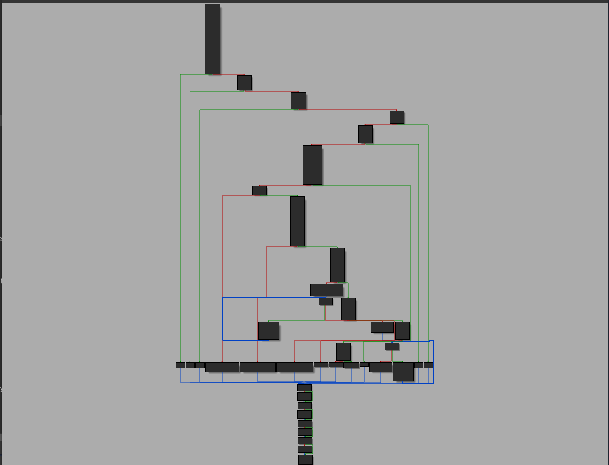
However, doing this PCB reversing hands on with an actual device is always more fun :). As the details of the PCB are difficult to get on these pictures, I'll use some visual elements to highlight our progress on identifying all the interesting parts!